design”")
ABL on “Printed circuit boards (PCBs) design”
Department: Electrical and Electronics Engineering
Year/Sem: II semester B.Tech and Diploma students
Activity: One day ABL Workshop
Title: ABL on “Printed circuit boards (PCBs) design”
Resource person/agency and affiliation: Mr. Sanam Agnihotri, Mr. Abrar Rja, AP, & Mr. Tapan Das Bairagi TA, Department of Electrical & Electronics Engineering, Mandsaur University, Mandsaur
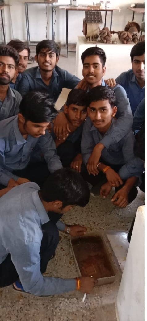
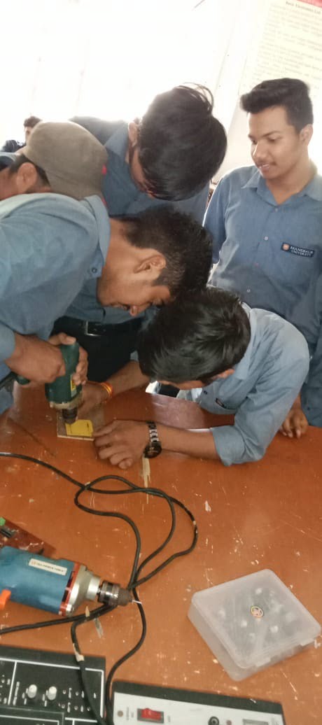
Brief description / remarks: The Department of Electrical & Electronics Engineering, Mandsaur University (M.P.) has organized one-day Activity-Based Learning (ABL) workshop on “Printed circuit boards (PCBs) design”. B.Tech and Diploma students of II semester actively participated in the aforesaid topic. The objective of the workshop was to make every student an expert in designing their own PCB board which would be very useful for developing their own projects. The workshop started with a PowerPoint presentation in which all the basic concepts of PCB design and electronic circuit fabrication on PCB were discussed.
The students were then familiarized with the more technical aspects of the PCB Designing: scrubbing, ironing, etching, drilling, and soldering. The circuit board is dipped into a chemical that removes the unnecessary copper from the circuit board. Etching helps in better circuit efficiency as there are now minimal chances of short-circuiting. Once the layout is ready on the circuit board, holes are drilled using a hand drill where the component wires can be placed in order to complete the circuit. The technical volunteers helped the students to get the components in the correct position for soldering.
Soldering was the most delicate and critical part of PCB designing. It joined the circuit board and the components with heat and soldering wire.
The PCB was finally ready to work. When batteries were attached it worked as a full-wave rectifier. The students were given assignments to practice what they learned in the workshop.
After attending this workshop students have expressed their capability of Designing Special purpose PCBs for any Electronics Project. This workshop will be helpful for students in the circuit development of their project work. Total of 24 students have participated in this workshop, where everyone has got a chance to work individually on a separate PCB.
Outcome: To make every student an expert in designing their own PCB board.
No. of participants: 24
Prepared by: Mr. Sanam Agnihotri, EEE Department
Verified and Submitted by (HOD/HOI): Mr. Virendra Jain, EEE Department